- 您现在的位置:买卖IC网 > Sheet目录313 > AT28C256E-15TI (Atmel)IC EEPROM 256KBIT 150NS 28TSOP
AT28C256
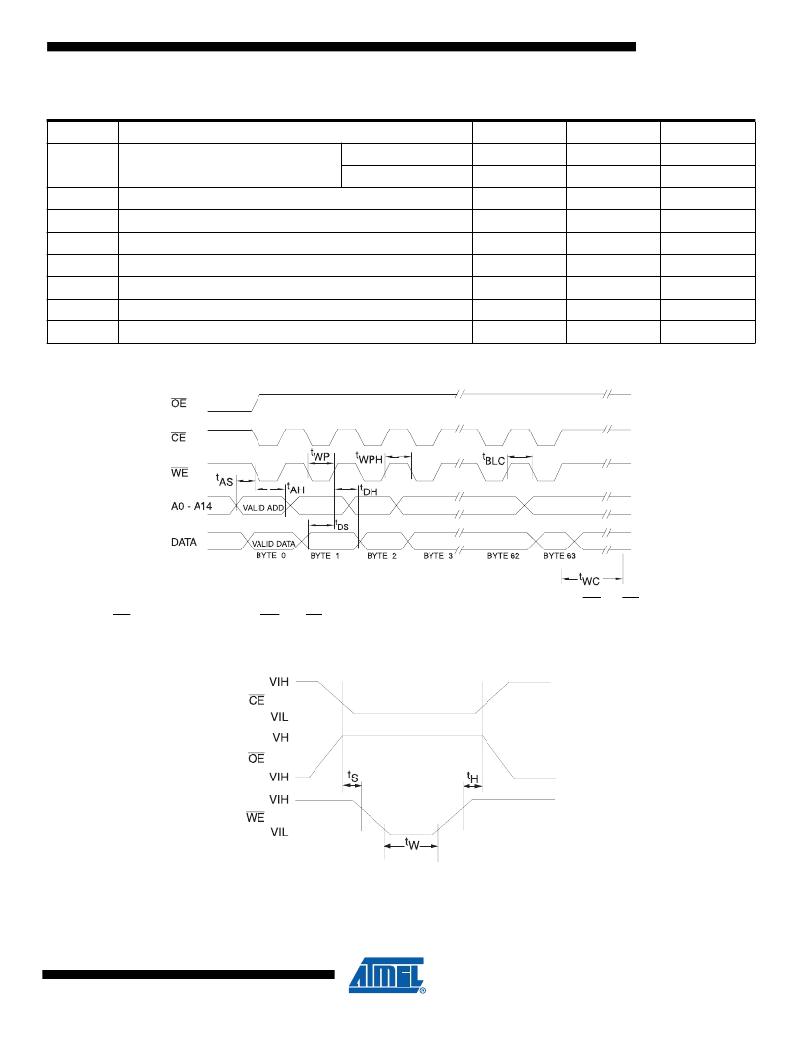
16. Page Mode Characteristics
Symbol
t WC
Parameter
Write Cycle Time (option available)
AT28C256
AT28C256F
Min
Max
10
3
Units
ms
ms
t AS
t AH
t DS
t DH
t WP
t BLC
t WPH
Address Setup Time
Address Hold Time
Data Setup Time
Data Hold Time
Write Pulse Width
Byte Load Cycle Time
Write Pulse Width High
0
50
50
0
100
50
150
ns
ns
ns
ns
ns
μs
ns
17. Page Mode Write Waveforms (1)(2)
Notes:
1. A6 through A14 must specify the same page address during each high to low transition of WE (or CE).
2. OE must be high only when WE and CE are both low.
18. Chip Erase Waveforms
t S = t H = 5 μsec (min.)
t W = 10 msec (min.)
V H = 12.0V ± 0.5V
9
0006M–PEEPR–12/09
发布紧急采购,3分钟左右您将得到回复。
相关PDF资料
AT28C64B-15SU
IC EEPROM 64KBIT 150NS 28SOIC
AT28C64E-25TI
IC EEPROM 64KBIT 250NS 28TSOP
AT28C64X-25SI
IC EEPROM 64KBIT 250NS 28SOIC
AT28HC256E-70TU
IC EEPROM 256KBIT 70NS 28TSOP
AT28HC64B-70TU
IC EEPROM 64KBIT 70NS 28TSOP
AT28HC64BF-12JU
IC EEPROM 64KBIT 120NS 32PLCC
AT28LV010-20JU
IC EEPROM 1MBIT 200NS 32PLCC
AT32UC3C-EK
KIT EVAL AVR32 UC3 MCU IND AUTO
相关代理商/技术参数
AT28C256E-15TU
功能描述:电可擦除可编程只读存储器 256K HI-ENDURANCE SDP- 150NS IND TEMP RoHS:否 制造商:Atmel 存储容量:2 Kbit 组织:256 B x 8 数据保留:100 yr 最大时钟频率:1000 KHz 最大工作电流:6 uA 工作电源电压:1.7 V to 5.5 V 最大工作温度:+ 85 C 安装风格:SMD/SMT 封装 / 箱体:SOIC-8
AT28C256E-15TU SL383
制造商:Atmel Corporation 功能描述:EEPROM PARALLEL 256KBIT 32KX8 5V 28TSOP-I - Tape and Reel
AT28C256E-15TU-T
功能描述:150NS, TSOP, IND TEMP, GREEN 制造商:microchip technology 系列:- 包装:剪切带(CT) 零件状态:在售 存储器类型:非易失 存储器格式:EEPROM 技术:EEPROM 存储容量:256Kb (32K x 8) 写周期时间 - 字,页:10ms 访问时间:150ns 存储器接口:并联 电压 - 电源:4.5 V ~ 5.5 V 工作温度:-40°C ~ 85°C(TC) 安装类型:表面贴装 封装/外壳:28-TSSOP(0.465",11.80mm 宽) 供应商器件封装:28-TSOP 标准包装:1
AT28C256E-15UC
制造商:未知厂家 制造商全称:未知厂家 功能描述:x8 EEPROM
AT28C256E-15UI
制造商:未知厂家 制造商全称:未知厂家 功能描述:x8 EEPROM
AT28C256E-15UM
制造商:未知厂家 制造商全称:未知厂家 功能描述:x8 EEPROM
AT28C256E-15UM/883
功能描述:电可擦除可编程只读存储器 256K HI-ENDURANCE SDP - 150NS
RoHS:否 制造商:Atmel 存储容量:2 Kbit 组织:256 B x 8 数据保留:100 yr 最大时钟频率:1000 KHz 最大工作电流:6 uA 工作电源电压:1.7 V to 5.5 V 最大工作温度:+ 85 C 安装风格:SMD/SMT 封装 / 箱体:SOIC-8
AT28C256E-15UM/883 SL815
功能描述:IC EEPROM 256KBIT 150NS 28PIN 制造商:microchip technology 系列:- 包装:托盘 零件状态:停產 存储器类型:非易失 存储器格式:EEPROM 技术:EEPROM 存储容量:256Kb (32K x 8) 写周期时间 - 字,页:10ms 访问时间:150ns 存储器接口:并联 电压 - 电源:4.5 V ~ 5.5 V 工作温度:-55°C ~ 125°C(TC) 安装类型:通孔 封装/外壳:28-BCPGA 供应商器件封装:28-CPGA(13.55x15.06) 标准包装:20
